Homebrew, open source, repurposed, hacked, software defined, open hardware

Wednesday 29 March 2017

ISO 3098 CAD compatible font support, dwarven rune, and Klingon support, in the gEDA PCB fork pcb-rnd

In keeping with the monthly feature release schedule for pcb-rnd, on April 1, 2017, the gEDA PCB fork pcb-rnd will release new features designed to enhance backwards compatibility, improve compliance with ISO  3098, and anticipate future needs of users.

The ASCII character set has been ported from the ISO 3098 compatible open font osifont to the new pcb-rnd polygonal glyph format, to allow its use in PCB layouts.

This complements the existing stroked default font, as well as the stroked Hershey Sans 1 Stroke Font, also available for use within pcb-rnd.

The commitment to ongoing support for legacy users has been cemented with the addition of a Runic font, believed to be popular among Numenoreans who, it is thought, continue to use awk, C89, and at times, scheme.

Looking forwards to future users, and in particular, the Treaty of Organia in 2267, a Klingon pIqaD HaSta font has also been ported to pcb-rnd.

pcb-rnd retains support for the traditional gEDA PCB font file format, as well as the new, more fully featured lihata (.lht) file format which supports lines, arcs and polygons within font glyphs.


Here's a screen shot of the exported gerber being viewed in the gerber viewer gerbv, showing dwarvish runes, Klingon, osifont, and the Hershey Sans One Stroke font.


The support for these fonts has been made possible by the multiple font support recently implemented in pcb-rnd, in addition to the newly implemented support for polygons within font glyphs in the new pcb-rnd lihata (.lht) file format used for both pcb layouts and font files.

Both stroked fonts and polygonal glyph fonts (.lht) are dealt with in the font browser window:


The new pcb-rnd file format even allows an individual refdes to have an individual font allocated, if required:


To join in on the fun, head on over and grab yourself a copy of pcb-rnd.

To convert truetype fonts into pcb-rnd compatible lihata font files, you'll need to use the Apache Batik utility ttf2svg to convert the desired glyphs to SVG glyphs.

These SVG glyphs can then be converted to a pcb-rnd compatible font file with the outlineFont2centrelineFont utility. The outlineFont2centrelineFont utility is still a work in progress, but it was used to generate the Klingon, Dwarven Rune and osifont files pretty quickly and easily. The outlineFont2centrelineFont README explains how to go about doing the conversion. All that remains to be done with it is automatic merging of inside and outside paths in truetype or svg glyphs (these were done manually for the fonts shown).

Over time, new fonts in legacy and/or lihata (pcb-rnd .lht) will be added to the new EDA tool agnostic repository, EDAkrill:

http://repo.hu/projects/edakrill/

The EDAkrill project is an effort to create a platform and toolchain agnostic repository of footprints, symbols, fonts and anything else EDA related.


Monday 20 March 2017

Converting inkscape paths to pcb-rnd and gEDA PCB layouts, lines and footprint elements

Inkscape is a powerful FOSS vector graphics tool that allows editing of complex paths which can then be exported to various formats.

Being able to export paths to PCB layout software is useful for a number of reasons, such as enabling custom or artisanal board outlines and tracks to be implemented, such as the following flying spaghetti monster (FSM) designed with pcb-rnd and FidoCadJ:


or allowing intelligent design of exotic footprints like the following touch pad example:


After looking at an Inkscape HPGL export module written by Aaron Spike, a pair of python modules were written, based on the Inkscape's HPGL exporter.

These extension scripts are available from:

https://github.com/erichVK5/inkscape2pcb

and the *.py and *.inx scripts need to be copied (you'll probably need sudo / superuser privileges) into your local inkscape extensions folder, i.e.

/usr/share/inkscape/extensions

After starting Inkscape up again, and creating a design...


...you should have the options to export to both gEDA PCB footprint (.fp) format, and to pcb-rnd layout (.lht) format available in the "Save As:" menu:


The paths in the layout are automatically flattened and converted to line segments in the exporter:

Here's the exported layout being viewed in pcb-rnd, the fork of gEDA PCB:


And here's the layout exported as a footprint, being viewed in gEDA PCB.


Naturally, KiCad users can use the same scripts to export footprint designs, since KiCad can import gEDA PCB footprint (.fp) natively.

There may be scope to improve the code by implementing export of solid polygons, but more needs to be learned about Inkscape's internal data structures first.

Support for specifying line thickness has also been added to the export dialog, and can range from 8mil (default) to 250mil (mil being thousands of an inch, a.k.a. thou, a.k.a. 254 microns, a.k.a. 0.254mm). This is a fairly sane range of values, but the thickness can always be changed in gEDA PCB or pcb-rnd if necessary.


The scripts have been tested with "px" as the default unit of measurement in Inkscape. One "px" maps to one mil in gEDA PCB and pcb-rnd; users will need to confirm that exported dimensions are maintained when exporting; if not, the dpi setting could be experimented with for scaling during export.

In closing, it should be mentioned that accurate geometry in Inkscape is most easily achieved by individually clicking on nodes, and then manually entering their required coordinates.

Wednesday 15 March 2017

Importing Mentor Graphics Design Capture netlists into gEDA pcb-rnd

In the continued effort to have pcb-rnd (the actively developed fork of the gEDA PCB layout tool) support additional import and export formats, the ability to import netlists from the Mentor Graphics Design Capture has now been added and tested.

Based on a set of example files supplied by a Mentor Graphics Design Capture user, import has been implemented following reverse engineering of the EDIF files supplied.

Of note, the importer does not use the old EDIF import code, relying instead on the s-expression parser library more recently developed for KiCad import.

The importer allows use of the native Mentor parts database, with a regex based translation table during import into pcb-rnd that translates Mentor's parts into pcb-rnd native footprint names. This can use any attribute of the input part and can generate the pcb footprint using parts of the input string,

e.g. there is a single rule that says if Part Name is Dummy_HDR 1x2 P:2.54mm, extract the "1x2" and the "P:2.54mm" sections and add attribute 

footprint=connector(1, 2, 2.54mm)

which is a valid pcb-rnd parametric footprint.

This feature allows those using the Mentor Graphics Design Capture for schematic design to then layout a PCB in pcb-rnd based on the exported schematic netlist. The supported export netlist format is a flattened EDF file.

Options for further development and improvements include attempts to import mentor footprints (i.e. geometry), and possibly attempts to import hierarchic netlists, with subsequent flattening within pcb-rnd.

Starting with a Mentor Graphics Design Capture schematic


the next step is to generate a netlist for importing by pcb-rnd based on the Mentor Graphics Design Capture schematic; the first thing is to open the utilities menu


In this menu, the option for exporting a netlist in EDIF format can be selected. In particular, the flattened schematic option must be selected:


If successful, an EDIF format netlist should be written to your filesystem:


The next step is to load the netlist file within pcb-rnd:


It is at this point the footprints should be seen on the layout, and connections can be viewed with the rats nest optimize 'o' button:


from here, PCB layout proceeds as usual, with, of course, the option of adding additional footprints with the insert 'i' command.


In closing, the pcb-rnd project is keen to enable a variety of workflows and foster interoperability between layout and design tools. If you have a preferred schematic design tool, or are considering a move away from an existing tool and would like to see the ability to import legacy designs, feel free to get in touch with the developers on irc.

Thursday 9 March 2017

Exotic and complex footprint creation for gEDA PCB, pcb-rnd and KiCad pcbnew using FidoCadJ

Sometimes there are complex or exotic footprints that need to be made which are most easily achieved with bezier curve, cubic spline and ellipsoidal features in addition to the usual rectilinear elements.

A good example of one such footprint came up on the Kicad forums; a contact pad for use with rubber dome pushbutton switches which have a conductive underside which shorts out the gap in the exposed pad:


The fairly symmetrical design and filleted features are a natural fit for the cubic bezier, ellipsoid and cubic spline support in FidoCadJ, the no nonsense 2D cross platform CAD package which now has an export module for exporting these design features as line elements in a gEDA PCB / pcb-rnd layout.

The design was fairly quickly prototyped in FidoCadJ at a scale that suited the features. It should be noted that on export, FidoCadJ allows a magnification factor to be provided to allow the design to be magnified or shrunken, so the 5mil grid in FidoCadJ never becomes a limitation.

The design was executed on the "circuit" layer in FidoCadJ, since this is the default layer, and when exported to gEDA PCB / pcb-rnd format by the export module, is exported to the rear silk layer with 10mil lines by default.


After creating the outline and the interlocking features with cubic splines and lines, the internal, open portions were hatched with additional lines to act as fill. Following this, the layout was exported to a gEDA PCB / pcb-rnd (.pcb) layout using a magnification ratio of 0.18, which generated a footprint of the desired dimensions (~ 6mm round):


The exported layout was then loaded in pcb-rnd, the fork of gEDA PCB. The same process would work with mainline gEDA PCB.


The layout can be flipped in pcb-rnd / PCB with the tab key, if the underside is to be viewed, as above.

For an essentially round design such as this, a more uniformly contoured outer margin can be achieved by using an encircling ellipsoid, and deleting un-necessary line segments. This was ultimately done in this case, to create a more uniformly rounded appearance than cubic beziers were able to achieve.

Looking at the line elements from the front, the elements were selected with Alt-A, and then Ctrl-C was used to copy them into the buffer:


This design has point symmetry, enabling the copied elements to be mirrored twice, or rotated, to complete the other half of the footprint. The buffer contents were mirrored Left-Right:


and the buffer was then mirrored Up-Down:


The transformed buffer elements are then placed where they belong, completing the basic design. Some of the "fingers" were lengthened a little to fine tune the spacing, and any residual gaps in the hatched areas were filled with additional lines:


At this stage, the elements can be moved from the bottom silk layer to the front copper layer. First of all, the top copper layer needs to be selected in the layer list in the left dialogue of the gEDA PCB / pcb-rnd screen. Once the intended layer is selected, Alt-A is used to select all of the elements, and then "Shift-M" is used to move the elements to the top copper layer:


At this point, a KiCad pcbnew user can simply use the "Save As" dialogue to save the layout in either KiCad legacy or KiCad s-expression format, at which point it can be loaded into pcbnew for further manipulation:


gEDA users keen to create a gEDA PCB / pcb-rnd compatible footprint can proceed to do so by again using "Alt-A" to select all of the elements, followed by "Ctrl-X" to cut the elements to the buffer. Ensure the cursor is over an appropriate centroid or origin for the planned footprint - in this case the centre of the element was chosen for the mouse pointer location when "Ctrl-X" was used:


Using the "Buffer" menu, the buffer contents can be converted to a footprint with "Convert Buffer To Element" command:


Which results in the new element (footprint):


At this point the element can be saved to a footprint file:


Here's the final result, a footprint being viewed in pcb-rnd:


The remaining work required for use with a netlist and design rules checking is suitable numbering of the overlapping pads, to end up with two distinct electrical groups of pads, numbered either pad "1", or pad "2".

In a complex footprint design like this (ultimately with 401 distinct pads!), this is most easily achieved by loading the footprint into a text editor and doing some search and replace on the consecutively numbered pads.

Alternative approaches to creating a footprint like this would include using pstoedit, or tracing outlines in a utility like inkscape, and then exporting in a format compatible with one's preferred PCB layout editor or an intermediate conversion utility.

The method described is efficient, and appears to be the quickest and least painful method for complex curve creation in footprints at present.

It is worth noting that FidoCadJ now has support for loading a background image, which, with suitable scaling of the image prior to use, can provide a background template for duplication with cubic bezier, cubic spline, line and ellipsoidal elements.

Tuesday 7 March 2017

Converting Eagle (.brd) layouts to gEDA PCB / pcb-rnd (.pcb) format

Eagle has been a popular CAD program in some parts of the electronics community for many years, thanks to its multi-platform support and fairly integrated, "one stop shop" offering.

Accordingly, many open hardware designs and community contributed footprints and symbols now exist as a result.

The issue that naturally arises is how best to leverage and extend existing community contributed IP in the form of schematic symbols, footprints and layouts.

For some time (since the advent of the Eagle XML file format) gEDA users (and by extension, KiCad users able to import gEDA footprints into their pcbnew layout tool) have been able to extract schematic symbols and footprints from Eagle library (.lbr) and board layout (.brd) files by using translate2geda.

The current limitations of this conversion pathway via translate2geda are

1) polygonal pads (albeit rarely encountered) in Eagle are not supported in gEDA footprints

2) board layout conversion has not yet been implemented, due to Eagle's frequent use of rotated footprints within layouts, necessitating some refactoring to allow this to work smoothly.

3) following on from 2), to convert symbols and footprints in a layout file (.brd), you need to rename it to a .lbr file before running it through translate2geda

Issues 2) and 3) are simply a matter of finding time to write more code.

Issue 1) will require extensions to pad definitions within gEDA PCB and pcb-rnd in due course.

So, how best to get an Eagle layout into a format for use within the gEDA ecosystem?


Update!!!!! - May 2017:

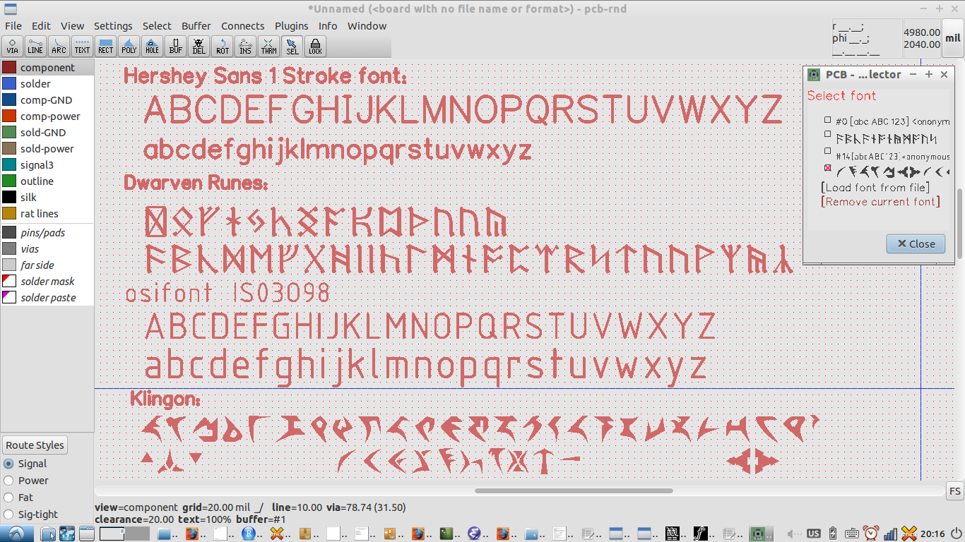
pcb-rnd now has native Eagle XML import support

Update!!!!! - December 2017:

pcb-rnd now has native Eagle Binary (V3, v4, v5) import support, as well as Eagle XML and Eagle Binary library (.lib) support

... and now back to our previous programming:

A fairly imperfect method is to find gerber files generated by Eagle, and use translate2geda to convert the gerber files into footprints for use as a template within gEDA PCB, pcb-rnd, or KiCad. It's simple enough to do:


Here's a converted layer one (.L1) gerber from the SM1000 codec2 smart microphone designed by Rick Barnich KA8BMA and David Rowe VK5DGR:


Although the converted gerber-as-footprint is not without uses, the biggest problem with it is Eagle's tendency to paint any gerber features with a raster of lines which is not

1) a simple track,
2) a round pad, or,
3) a square pad

This can be seen in the following screenshot where a number of features have been highlighted


As the good people at UCAMCO hath doth verily spake unto us in their "open letter on standard gerber"

"Consider this happening not just once, but maybe hundreds of times, and in different sizes, across a densely populated PCB, and it quickly becomes obvious that painted features are every CAM engineer's nightmare"

As well as resulting in a bloated design description file (and gerbers), this will limit the usefulness of gerbers converted in this way when it come to snapping items to features in the footprint.

The other limitation is the difficulty translate2geda encounters in trying to identify what is a pad and what isn't during conversion; non square and non round flashed polygons aren't necessarily going to appear on the layout as a pad with heuristics currently implemented in translate2geda.

At present, a more workable pathway is to take advantage of the (FOSS) KiCad project's layout editor, pcbnew, which is able to import Eagle XML layouts.

Here's the same SM1000 layout being viewed in pcbnew:


And here is the file dialogue being used in pcbnew to save it in pcbnew's s-expression layout format (.kicad_pcb).


Once saved in a kicad format (.kicad_pcb), the layout can then be loaded into pcb-rnd, which can load these layouts natively:


pcb-rnd is a fork of the gEDA project's pcb layout tool, "PCB". From there, you can proceed with business as usual.

In addition to the open hardware SM1000 design, the workflow was tested and pcb-rnd's s-expression import module refined with another example, this time from Adafruit's git repo, namely, an
Adafruit-PiTFT-3.5-Plus-PCB touch screen PCB layout


Concluding remarks:

An effective method now exists for sharing open hardware designs and community contributed design elements in Eagle's XML format with the gEDA ecosystem.

gEDA toolchain users now have multiple options available for extracting design information from Eagle generated gerber files, Eagle board layout files, and Eagle library files with the techniques outlined.


Caveats / fine print:

These arise primarily from the non-surjective and non-injective mapping of features when translating from one EDA tool to another....

1) As previously discussed, polygonal pad features will not be converted into gEDA compatible footprint features

2) text size, kerning, justification and styles will be altered somewhat during translation through various EDA formats

3) KiCad has some peculiar interactions between polygonal zones and via/pin definitions/thermal properties, meaning that these features need to be checked carefully in a converted board.

4) KiCad tends to specify pullbacks from polygonal zones, which are not a feature of polygonal entities in gEDA.

5) KiCad doesn't necessarily translate an imported Eagle layout into a sensible location within the KiCad layout, so you need to select the layout and move it into the layout's bordered area before saving it in .kicad_pcb format. Here's the SM1000 layout before being moved in KiCad's layout window.


6) converted files are likely to have in excess of 16 layers, which will require a recent build of pcb-rnd, or a recompiled version of mainline PCB with support for an increased number of layers with modifications to the relevant header files.

Failing that, and probably the simplest layer limitation workaround for those disinclined to recompile, is to simply cut and paste the contents of each layer of interest with a text editor into the relevant layer sections of an existing empty layout (.pcb) file, along with the section defining the footprints prior to the layer definitions. If, after doing this, nothing appears in your layout, you need to resize your layout in the preference dialogue; the design is probably sitting outside of the board's defined area...


Wednesday 1 March 2017

On the fly parametric footprint creation and editing in the pcb-rnd PCB layout editor plus gedaymbols support.

pcb-rnd is a fork of gEDA's PCB layout editor, and aims to continue adding features that improve functionality and improve interoperability with other FLOSS EDA tools and leverage existing FLOSS EDA ecosystem resources.

Recent improvements to pcb-rnd include the ability to fine tune footprint parameters on the fly, even while working on a PCB layout, in an intuitive and simple to use parametric feature editing dialog window.

The footprint insertion dialog is invoked by pressing the "i" key while editing a layout. In this respect, element insertion remains much the same as in mainlline gEDA PCB.

Unlike mainline PCB, the pcb-rnd user has the ability to then browse the local filesystem libraries, specify and edit a parametric footprint, or retrieve a footprint from a web based repository if it has been specified in the preferences.

Here's a resistor being specified parametrically for a layout being edited:


Here's a BGA footprint being specified on the fly:


Here, a standard BNC footprint is being added from the local library residing in the local filesystem: 


And here's a parametric DIP socket being specified on the fly in the parameter editing window:


A fatter than usual DIP has been created and placed on the layout:


In addition to the options of standard, inbuilt footprint libraries, and parametric footprint creation, pcb-rnd has had the ability to retrieve symbols from web repositories for some time.

Once a compatible web based repository has been specified, pcb-rnd checks for updates and caches a list of the available footprints whenever it starts up.

Here's a nixie tube footprint retrieved from gedasymbols.org. The nixie tube footprint was originally converted from a KiCad library, if memory serves correctly:


Importantly, any of the parameters generated interactively can also be embedded as footprint attributes in netlists exported by schematic editors, allowing parametric footprints to be specified from the schematic for automatic inclusion in the new layout.

A simple example for gschem, the gEDA project's schematic editor, would be the following attribute for a resistor:

footprint=acy(300)