Homebrew, open source, repurposed, hacked, software defined, open hardware

Tuesday, 6 June 2017

Using existing pcb layouts as footprint element libraries in pcb-rnd

Recent additions to the modular import and export code in pcb-rnd have allowed for existing pcb layouts to now be used as footprint element libraries.

This is likely to be of use in computer labs, organisations maintaining multiple seats with version controlled design elements, and also handy for distributing design element libraries generally.

The preferences dialogue allows various sources of design elements to be specified, such as wget for gedasymbols.org, the EDA agnostic edakrill repository, local directories, scripted elements in pcblib, and now board layout files.

As shown in the screen shot, the path to the file is prepended with

    board@


Here is a simple example of the "i" insert element dialogue box, with a native pcb-rnd lihata (.lht) board layout being used as a source of footprints on a new layout:


The code allows any supported board format to serve as a source of design elements; here is another example of the insert element dialogue, this time using a board layout in gEDA PCB's (.pcb) format:


Testing of this new feature with more exotic board types would be appreciated, such as Kicad and Eagle XML layouts, so that any corner cases can be identified and dealt with.


Wednesday, 31 May 2017

New routing options in pcb-rnd including angle-preserving rubber band and curvy knees on silk and copper

Recent refinement of the pcb-rnd rubber band code has allowed a radius to be specified (other than the default of zero radius) when routing tracks.

The key commands:

    Alt+c

and

    Alt+shift+c

are used to alter the radius used for bends in the track being routed. These settings can also be adjusted in the preferences dialog.

With this capability, free-form, artistic trackwork is easier without needing other vector drawing utilities for copper, silk and outline layer features.

The following creation was done quickly and easily in pcb-rnd without needing to use any svg or similar vector artwork as a preliminary source of contours, thanks to the new radiused rubber band feature:


DJ Delorie's teardrop code is a longstanding plugin available for both pcb-rnd and gEDA PCB. The teardrops() plugin is enabled in pcb-rnd by default.

Beyond the merely artistic, this "banana mode" ability is also of interest to those routing RF and high speed signals on their PCB.

DRC can auto enforce clearances around other features while rubber banding as well, as seen in the videos below.

Here is the angle preserving rubber band mode.


Here is the bendy knee support in action.


And here is the teardrop effect being applied with the ":" key, followed by the

   teardops()

command.


Monday, 8 May 2017

pcb-rnd now has native support for Eagle XML (.brd) PCB layout import

Taking advantage of the modular import/export infrastructure in pcb-rnd that was first exploited for KiCad s-expression and KiCad legacy layout support, an IO module has recently been developed to allow native import of Eagle XML (.brd) layout files.

Update!!!!! - December 2017:

pcb-rnd now has native Eagle Binary (V3, v4, v5) import support, as well as Eagle XML and Eagle Binary library (.lib) support.

This is a significant milestone as it allows recovery of archived Eagle XML and binary format designs by existing or previous Eagle users, as well as facilitating continued distribution and use of open hardware designs originally designed in Eagle and then shared with the maker/OSHW community.

Here is an example, an Eagle XML format OSHW design, namely, the Replicape A4, from:

https://github.com/moto-timo/Replicape/blob/master/PCB_rev_A4/Replicape_A4.brd

loaded directly into pcb-rnd:


Further testing is needed to refine text scaling and validate element placement/rotation routines.

Users are invited to experiment and make feature requests or report any issues.

Sunday, 16 April 2017

Bitmap import now supported by pcb-rnd, including Easter eggs


Support for parametric footprints within pcb-rnd, the gEDA PCB fork, now allows on the fly insertion of any graphic file type as a silkscreen bitmap, including easter egg depictions, of course, that are supported by the netpbm package that the bitmap() script depends on.

At this point in time, netpbm supports:

bmp, fiasco, fits, gem, gif, jpeg, palm, ps, rast, rle, sgi, sir, tiff, xwd, zeiss, png

which means that any of these image formats can be inserted, on the fly, into a pcb-rnd PCB layout as a bitmap.

The bitmap() script can be found on the edakrill repository.

The script files need to be installed in the search path for parametric footprint elements, i.e.

    pcb-rnd/trunk/pcblib/parametric/

The footprint insertion dialogue is invoked with the usual "i" command, at which point the path to the image can be entered into the bitmap() footprint dialogue as follows, along with pixel size details:


At which point the graphic is turned into an element in the buffer:


Which can then be placed on the layout:


This is a somewhat simpler way of inserting images than other workflows including the use of pstoedit or image2footprint, previously described, which are used standalone to generate the layout element for subsequent insertion into the PCB layout.

Image size and resolution should be kept sensible, as the resulting footprint silkscreen elements will get quite big and bloat a layout if excessively high resolution images are used, and may encounter manufacturer limitations with minimum silkscreen dimensions, i.e. less than 6 or 8 mil, depending on the manufacturer.

Sunday, 9 April 2017

Line, Polygon and Arc objects now supported in pcb-rnd font glyphs

Further work on multiple font support in pcb-rnd  handling has  led to the addition of support for not just polygons within glyphs, but also arc objects. Until now, gEDA PCB and pcb-rnd have been limited to line objects only within glyphs.

pcb-rnd's   :FontEdit   code has been updated to allow arcs to be edited and saved by those wishing to create their own fonts or modify existing fonts. Those familiar with   :FontEdit   and   :FontSave   will appreciate the ability to use arcs when creating rounded glyphs in a new font:


Fonts with arc objects can be saved as standalone font files in pcb-rnd's new lihata (.lht) file format. These font files can then be easily shared, and loaded into a pcb-rnd layout with the font load window (CTRL-SHIFT-F).

Here is an example of an arc based default font, (default_arc.lht) alternative to the legacy default_font:


Multiple fonts can be used simultaneously in pcb-rnd; here is the traditional default_font shown above the arc based example font:


Advantages of the new arc-based font are more compact gerber export, and more compact font description files, since three or more lines can be replaced with just one arc description.

The traditional default_font remains the default font in pcb-rnd, but users are free to try out the example arc based font in the trunk/font directory in addition to the traditional default_font in the trunk/src directory if keen.

The default_arc.lht example arc based font is a working example of the new font file syntax, and can be referred to by those keen to design their own fonts.

Those crafting new font files in lihata (.lht) format should find the format quite human parseable, and need only note that hashes of the form

  ha:j {

  }

which contain details for a particular glyph, in this case, "j", need have the character escaped if the hash refers to one of the following ASCII chars:

  {     }      \      :      ~     ;     =     &     #

and also ASCII 32, the space character, for lihata parsing to behave properly.

Examples of how to do this can be seen in the default_arc.lht example file, either by pulling down an svn copy of the repo, or browsing the repo online at

http://igor2.repo.hu/cgi-bin/minisvn.cgi?cmd=browse&repo=pcb-rnd&path=trunk

pcb-rnd also supports multiple font editing options with the updated   :FontEdit   code via the miantenance menu, allowing editing of the current font within a layouts, or editing of fonts residing on disk:


Thursday, 6 April 2017

QR code and code128 barcode support for PCB layouts now in pcb-rnd, the gEDA PCB fork

As part of the extensible parametric footprint support in the gEDA PCB fork, pcb-rnd, support for QR-codes and code128 barcodes on pcb layouts has been implemented.

The necessary awk scripts can be obtained from the EDAkrill repository, http://repo.hu/projects/edakrill/

Installation of the qrencode library on the machine running pcb-rnd is required.

A QR-code can be instantiated with a footprint attribute like:

 qr(hello world, 37.00mil)

or

 code128(hello world, 0.001m)

embedded in a netlist exported from a schematic. The dimension refers to the pixel size.

Of note, parametric footprints scripts are able to parse the usual dimension suffixes, i.e. mm, mil, dmil, cmil, in, um

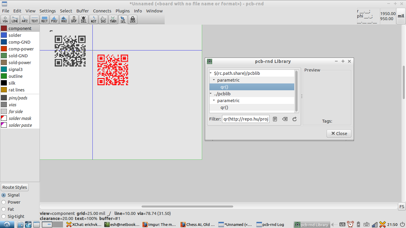
Alternatively, and somewhat simpler, is to simply use the "i" element insertion dialogue within the layout editor to provide the text and pixel dimensions for insertion as a QR-code, i.e.


The QR-code text and pixel size can be selected, along with either high or low level error coding:


After this, the QR-code can be placed on the layout, like any footprint element:


and here's the QR-code with a bit of zoom applied...


Similarly, a code128 format barcode can be instantiated with a footprint attribute like:

  code128(hello world, 1000.00um)

or

  code128(hello world, 0.1cm)

or by instantiating the "i" insert element dialogue, i.e.


after the height, barcode bar width and text are defined, the element can be placed on the layout:


Like any footprint element, the text label can be resized and moved.


A footprint created this way can be saved from the buffer either before placement, or after copying into the buffer, if a standalone footprint is required, i.e. for importing into KiCad or frequent use.

Of note, the pairs of awk scripts that implement the qr() and code128() parametric footprints need to be placed in pcb-rnd's

   trunk/pcblib/parametric

directory, and can serve as templates for your own modifications or alternative parametric footprint types which will automatically show up in the element insertion dialogue on restarting pcb-rnd, if placed in this directory.

Over time, additional user contributed awk scripts for parametric footprints will also be available on edakrill, the new platform and  format agnostic EDA repository.

Wednesday, 29 March 2017

ISO 3098 CAD compatible font support, dwarven rune, and Klingon support, in the gEDA PCB fork pcb-rnd

In keeping with the monthly feature release schedule for pcb-rnd, on April 1, 2017, the gEDA PCB fork pcb-rnd will release new features designed to enhance backwards compatibility, improve compliance with ISO  3098, and anticipate future needs of users.

The ASCII character set has been ported from the ISO 3098 compatible open font osifont to the new pcb-rnd polygonal glyph format, to allow its use in PCB layouts.

This complements the existing stroked default font, as well as the stroked Hershey Sans 1 Stroke Font, also available for use within pcb-rnd.

The commitment to ongoing support for legacy users has been cemented with the addition of a Runic font, believed to be popular among Numenoreans who, it is thought, continue to use awk, C89, and at times, scheme.

Looking forwards to future users, and in particular, the Treaty of Organia in 2267, a Klingon pIqaD HaSta font has also been ported to pcb-rnd.

pcb-rnd retains support for the traditional gEDA PCB font file format, as well as the new, more fully featured lihata (.lht) file format which supports lines, arcs and polygons within font glyphs.


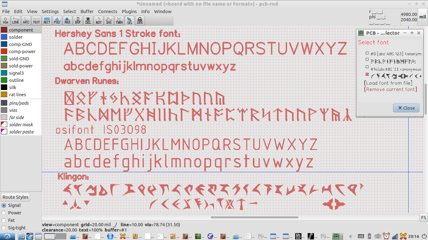
Here's a screen shot of the exported gerber being viewed in the gerber viewer gerbv, showing dwarvish runes, Klingon, osifont, and the Hershey Sans One Stroke font.


The support for these fonts has been made possible by the multiple font support recently implemented in pcb-rnd, in addition to the newly implemented support for polygons within font glyphs in the new pcb-rnd lihata (.lht) file format used for both pcb layouts and font files.

Both stroked fonts and polygonal glyph fonts (.lht) are dealt with in the font browser window:


The new pcb-rnd file format even allows an individual refdes to have an individual font allocated, if required:


To join in on the fun, head on over and grab yourself a copy of pcb-rnd.

To convert truetype fonts into pcb-rnd compatible lihata font files, you'll need to use the Apache Batik utility ttf2svg to convert the desired glyphs to SVG glyphs.

These SVG glyphs can then be converted to a pcb-rnd compatible font file with the outlineFont2centrelineFont utility. The outlineFont2centrelineFont utility is still a work in progress, but it was used to generate the Klingon, Dwarven Rune and osifont files pretty quickly and easily. The outlineFont2centrelineFont README explains how to go about doing the conversion. All that remains to be done with it is automatic merging of inside and outside paths in truetype or svg glyphs (these were done manually for the fonts shown).

Over time, new fonts in legacy and/or lihata (pcb-rnd .lht) will be added to the new EDA tool agnostic repository, EDAkrill:

http://repo.hu/projects/edakrill/

The EDAkrill project is an effort to create a platform and toolchain agnostic repository of footprints, symbols, fonts and anything else EDA related.