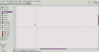
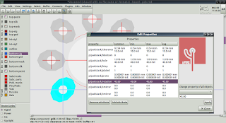
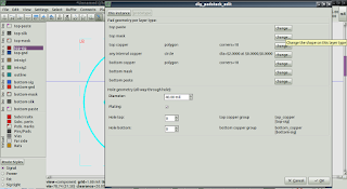
The new padstack support in pcb-rnd supports arbitrary copper shapes and will replace the roles of distinct pin, pad, hole and via features.
To
allow users to edit these shapes for custom padstack copper features, a
new copper shape tool can be invoked with the :shape() command.
As
a worked example, a footprint for a B7G thermionic valve, a.k.a. tube,
will be produced from scratch, using the following device data:
We
begin by creating a hole for the centre of the footprint. We do this by
selecting the via tool and placing a via at a suitable location in a
new layout:
We place the via at (1000,1000) mil to simplify subsequent calculations:
We now select the via by clicking on it:
We now use CTRL-x to cut the via to the buffer
We now use the "Convert buffer to padstack" menu item to convert the via to a padstack:
Having done so, we click to place the new padstack on the layout:
We now click on the padstack to select it:
Having selected the padstack, we can now invoke the padstack editor with the :padstackedit() command:
this produces the following window:
if we click on the prototypes tab, we can inspect and edit the characteristics of the padstack we have just created from the via. We begin by setting the diameter of the hole to 0.222 in, based on the electron tube data sheet. Note that pcb-rnd understands common dimensional
suffixes, like 'mm', 'nm', 'in' or 'mil':
We also note that there are superfluous copper shapes defined for the top, bottom and inner layers. This is to be expected, given that we made the padstack from a via. We can click on the "change..." button for the top layer copper shape to edit it:
We can delete the copper shape for this layer, and do the same for the other defined copper layer shapes. The final result is a padstack property window showing no copper shapes defined, as required for a simple hole:
Having sorted out the central hole for the footprint, we now use the via tool to place a new via that is to become the padstack used for the pins of the B7G tube.
Having done so, we select the via and with the top layer selected, we type ':shape()' to invoke the copper polygon shape tool...
which
brings up the following window, allowing us to create a polygon that
will become a pad for the padstack. We begin by editing the horizontal
and vertical dimensions:
We
then choose a more rounded pad shape, by increasing the number of
corners to 10. Note that the shape() dialogue also supports the creation
of round, rounded corner rectangle ("roundrect") and rectangular pads.
Polygonal pads were chosen for this particular footprint because of the
radial spacing and symmetry of the pins on the tube:
Having done this, we use the shape() tool to create another pad for our padstack on the bottom copper layer:
Having added to polygonal pads centred on our via, we use the selection tool to select the three features
which we then cut to the buffer with CTRL-x
and proceed to convert to a padstack with the "Convert buffer to padstack" menu item:
We now place the padstack in an intended location, based on the datasheet for the tube:
We continue pasting the padstack from the buffer in the remaining pin locations, based on the dimensions from the data sheet:
We place the easy 90 degree spaced pin padstacks first:
And then do a bit of trigonometry to calculate the positions of the remaining pins and place padstacks in these locations too:
Having positioned the padstack in the necessary locations, we review the work thus far:
Our
next job is to rotate the various padstacks as necessary. We do this by
selecting each padstack in turn, using CTRL-e to invoke the property
editor, and altering the rotation value as required. Applying -45
subtracts 45 degrees from the current value:
Similarly, applying 45 to the rotation, adds 45 to the rotation value:
Likewise, additional rotation of 90 is applied to the top pin:
almost done, we add 45 degrees rotation to the bottom left pin:
and we finish by subtracting 45 degrees rotation from the bottom right pin:
We now select the arc tool....
And now select the top silk layer to draw an arc to denote the outline of the tube, based on the datasheet:
A simple way to do this is to draw a 90 degree arc as follows:
after
this, select the arc and invoke the property editor with CTRL-e to
define the desired value for delta, to create a circle. The other way to
do this is to simply click on the end of the arc and then drag the end
of the arc around until a circle is formed.
The text tool is now used to add a text label to the footprint.
Having completed the components required for the thermionic valve, the set of features is selected:
and CTRL-x is then used to cut the selection to the buffer. It is important to note that the location of the mouse when CTRL-x is used determines the origin of the resulting footprint. In this case, the cursor is snapped to the central hole before using CTRL-x, to give a footprint origin centred on the hole:
With the features now cut to the buffer, we can convert the buffer contents to a subcircuit with the menu item "Convert buffer to subcircuit":
We now see the red, thin dashed line surrounding our new footprint, labeled 'U0':
All
that remains is to number the terminals of the footprint. This is done
by hovering over a terminal, and typing 'n', which brings up a window
allowing a label to be specified. Each of the pins is numbered this way.
The numbering can be checked afterwards by hovering over each pin in turn, and noting its properties:
We now inspect the completed footprint from the top
We inspect it from below, by hovering over the centre of the footprint and using SHIFT-Tab to flip the board
We
return to the front view and see the effect of turning off
'Subcircuits' visibility, which toggles the display of the dashed thin
red outlines of subcircuits
We also see the effect of turning off
'Padstack marks' visibility, which toggles the display of the red padstack crosshairs
We now undertake the final task of setting an appropriate solder mask clearance for the padstacks.
We select the footprint:
We now invoke the padstack editor with :padstackedit() to get the following window:
we click on the prototype tab to view the properties of the padstack upon which all seven pins are based
In
this window, we see that there are no solder mask properties. We click
on "change..." and automatically generate a mask shape for the top
layer:
We now do the same for the bottom layer mask properties:
and automatically generate a mask opening:
While
it is open, we also use the padstackedit() window to confirm, or change
if necessary, that the pin holes have 40mil (0.040 in) diameters, as
per the data sheet. Obviously, at this point, individual designers might
opt for larger holes to allow some room for variation in manufactured
pin sizes and PCB manufacturing tolerances.
Similarly, if a copper pad shape has been defined for the top layer, the padstackedit() window can be used as a short cut to copy the shape to the bottom layer, eliminating the need for manually creating a bottom layer shape for inclusion in a padstack being created from scratch.
We finish by toggling the solder mask layer, and seeing the resulting solder mask clearances:
In closing, we note that the preceding example demonstrates multiple new features in pcb-rnd:
1)
Footprints are now subcircuits, rather than a distinct hardwired
"element" type. This means that a text label or text labels are now
possible within footprints, and also that an arbitrary polygonal pad is
possible on any given layer, rather than the more limited options in the
past of SMD (rectangular), round pins and square through hole pins.
2) the shape() tool is a quick and easy way to build common padstack copper features.
3)
we saw how pcb-rnd can use a padstack prototype which can then be
copied and modified as needed within a footprint. In this case, the one
prototype padstack sufficed for all seven pins, the only differences
between them being rotation.
4) holes are now just a type of padstack, and are no longer a unique or distinct feature type.


Excellent Blog. I really want to admire the quality of this post.
ReplyDeletee-waste recyclers in India
Thanks for the wonderful information. Keep it up.
ReplyDeleteE-waste recycling company in chennai
Nice post and good to know about building footprints. Thanks for sharing and you can also check e waste recyclers in bangalore
ReplyDeleteNice post and good information. Thanks for sharing and you can also check plastic waste management
ReplyDeleteWelcome to Automatic Swing Gates Repair London ! Our team of experienced mechanics are here to help you with all your swing gate repair needs. From fixing broken hinges to installing new gates, we can handle it all! Give us a call today and let us help you get your swing gate back up and running like new in no time!
ReplyDeleteWe're excited to announce that our Shutter Repair Service in London is now available! With our experts on hand, we can quickly and easily repair any type of shutter.
ReplyDeleteAutomatic door store London provides sliding doors, scaffold gates, automatic sliding doors, automatic swing doors, and automatic doors. Choose from a huge range of sizes and styles with quick support and reasonable prices.
ReplyDeleteAdditionally, UK Roller Shutter provides Section Overhead Doors, which are compact and offer high-level insulation with a pleasing finish. These doors are perfect for situations where space is limited and a high level of insulation is required.
ReplyDeleteUK Roller Shutter provides High-Security Roller Shutters for maximum protection against intruders and vandalism. Ideal for commercial, industrial, and residential properties, our durable shutters offer strength, reliability, and automation options. Contact us for expert installation and maintenance services.
ReplyDeleteUK Roller Shutter specializes in Sectional Overhead Doors, offering superior insulation, security, and space-saving design for industrial and commercial properties. Our high-quality doors ensure smooth operation, durability, and energy efficiency. We provide expert installation, maintenance, and repairs across the UK. Contact us today for reliable sectional overhead door solutions!
ReplyDeleteUK Roller Shutter offers Insulated Roller Shutters designed for energy efficiency, noise reduction, and enhanced security. Our high-quality shutters help maintain indoor temperatures while providing strong protection for homes and businesses. We specialize in installation, repairs, and maintenance. Contact us today for reliable and durable insulated shutter solutions!
ReplyDeleteUK Roller Shutter specializes in steel roller shutters, providing maximum security, durability, and weather resistance for businesses. Ideal for commercial and industrial properties, our robust shutters protect against theft and vandalism while ensuring smooth operation. Trust our expert installation and maintenance services. Contact UK Roller Shutter for reliable security solutions!
ReplyDeleteUK Roller Shutter offers perforated roller shutters, combining security with visibility and ventilation. Ideal for shops and commercial spaces, they provide protection while allowing light and airflow. Durable and stylish, our shutters enhance storefront appeal. Contact for expert installation and customization!
ReplyDeleteThis comment has been removed by the author.
ReplyDeleteUK Roller Shutter provides high-quality Fire-Rated Roller Shutters, offering superior fire protection for commercial and industrial properties. Designed to contain fire and smoke, these shutters enhance safety and compliance. We offer expert installation and maintenance. Contact UK Roller Shutter for reliable fire-rated shutter solutions today!
ReplyDeleteProtect your farm and equipment with UK Roller Shutter’s heavy-duty agricultural roller shutter doors. Designed to withstand harsh outdoor conditions, our weatherproof, galvanized steel shutters offer secure, low-maintenance access for barns, grain stores, and machinery sheds. Choose manual or automated operation for hassle-free durability. Built for farming. Built to last.
ReplyDeleteUK Roller Shutter offers professional roller shutter installation services for commercial, industrial, and residential properties. Our expert team ensures precise fitting, long-lasting durability, and enhanced security with every installation. We provide a wide range of shutter styles to suit your needs and budget. Trust UK Roller Shutter for reliable, efficient, and customised roller shutter solutions that protect your premises while maintaining a clean, modern appearance across London and beyond.
ReplyDeleteThis comment has been removed by the author.
ReplyDeleteUK Roller Shutter is a trusted fire rated rolling shutter manufacturer, providing high-quality fire-resistant solutions for industrial, commercial, and residential properties. Our shutters are designed to withstand extreme heat and contain fire, helping protect lives and property. Built to meet strict safety standards, they combine durability with reliable performance. Choose UK Roller Shutter for expertly engineered fire rated shutters tailored to your building’s safety and compliance requirements.
ReplyDeleteUK Roller Shutter offers expertly crafted Perforated Roller Shutters that combine security with visibility and ventilation. Ideal for retail stores and commercial premises, our shutters allow clear product display even when closed, enhancing storefront appeal. Built from durable materials and designed for smooth operation, our perforated shutters provide both protection and style. Choose UK Roller Shutter for reliable, modern solutions tailored to meet your business’s safety and presentation needs.
ReplyDelete