Homebrew, open source, repurposed, hacked, software defined, open hardware

Tuesday, 21 February 2017

Multiple font support now available in pcb-rnd

Modifications to the pcb-rnd core, along with the new lihata (.lht) file format, have allowed multiple font support to be implemented relatively quickly.

Fonts used in a layout are saved in the lihata file format file, but not if the layout is saved in the current gEDA PCB (.pcb) format.

The multiple font support leverages previous work done converting Hershey format fonts sourced from the open source and open hardware EggBot platform.

The translate2geda utility can now batch convert the hersheydata.py font archive used by the EggBot. This has made around 50 fonts available for use.

The fonts are managed with a font selector window:


After loading and selecting a font, it can then be used:


Fonts can also be specified for element text attributes, i.e. the RefDes, since element text attributes in the lihata file now include a font ID, allowing a RefDes to have something other than the default font used for rendering:


It should be noted that any particular font is still subject to a 127 char symbol space limit.

Mapping for Greek and Cyrillic is phonetic, and the Hebrew font adheres to a common keyboard mapping.

Apologies to any fluent Greek, Russian or Hebrew speakers who might take exception to Google Translate's advice during the making of the screenshot!

I expect that the Greek font should come in useful for "mu" and "Omega" in particular, no matter what the local language is.

The new font support is available from the pcb-rnd svn.

Enjoy responsibly!!

P.S. For those unaware, https://github.com/erichVK5/FootprintTextForPCB
can be used for rendering text labels within footprints being created for use within both gEDA PCB and pcb-rnd.

Monday, 20 February 2017

Importing Kicad eeschema netlists into gEDA pcb-rnd

Taking further advantage of the gEDA PCB fork pcb-rnd's modular architecture, a new import module to allow KiCad Eeschema netlists to be imported has been developed.

A fundamental motivation behind these import/export efforts is to grow the FLOSS EDA ecosystem, by enabling greater sharing of existing efforts within the intellectual commons.

The modularity of pcb-rnd is such that a sample pack consisting of a schematic, screenshot and exported netlist, is usually sufficient to implement a new import module.

This was done for KiCad's Eeschema, and an import module was soon working.

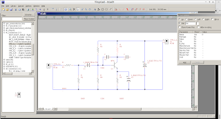
Here's an example schematic in Eeschema, the schematic editor used by KiCad:


Here's the netlist export dialog being launched:


The default netlist export format is selected:


And after using the file:import menu item in pcb-rnd:


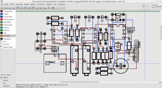
We get the new layout, and after rearranging, end up with:


Although the gEDA project's schematic editor, gschem, has powerful features such as arbitrary numbers of component attributes along with flexible and customizable netlist export options, there are likely to be existing designs or prospective gEDA users who would like to bring their existing designs with them.

The Kicad Eeschema import plugin is now available and enabled by default in the svn, and is expected to be in the next formal pcb-rnd release.

Further import plugins are planned for other schematic layout tools. If you have a tool you'd like to use with pcb-rnd, get in touch at http://repo.hu/projects/pcb-rnd/ and if it isn't a closed binary format, we should be able to make it happen pretty quickly.

Friday, 10 February 2017

Importing TinyCad schematics into gEDA pcb-rnd

As previously discussed, the gEDA PCB fork pcb-rnd has a modular architecture allowing import and export modules to be developed quickly.

Furthering the latest development efforts aimed at increasing the number of schematic layout tools that pcb-rnd can obtain netlists from, a new module has been written to allow netlists from the FOSS schematic editor TinyCad to be imported.

TinyCad is a windows application that runs quite happily on Linux under wine.

The gEDA project's schematic editor, gschem, continues to be a powerful, flexible and extensible schematic editor, but guile library availability on windows has at times lagged that on *nix, making alternatives to gschem valuable.

The import module is able to import a TinyCad netlist exported from TinyCad in TinyCad's own plain text netlist format.


The TinyCad netlist file (designName.net) contains enough information to allow pcb-rnd to populate a new layout with associated connection data.

TinyCad is quite flexible, and allows a footprint attribute, i.e. a "Package", to be associated with a component.

This is done easily by clicking on a component to make the attribute inspector appear


At which point a standard pcb-rnd compatible package can be specified in the window, i.e. 1206 for an SMD resistor:


The same design used for the LT-Spice netlist import example has been used for this example, to allow comparisons to be made.


Clearly, TinyCad is much more suited to an easy schematic -> pcb-rnd workflow than the current version of LT-Spice tested (v4).

Having exported the TinyCad plain text netlist from TinyCad, the next thing is to start pcb-rnd.

In pcb-rnd, the netlist can be imported, either with a command

:LoadTinycadFrom(/home/user/path/to/design.net)

or via the file menu:


The parts and connections (rat lines) will then appear


the parts can then be selected and dispersed


and then re-arranged into a nice grouping, ready for routing.


So, we see we end up with much the same result as that achieved with LT-Spice netlist import, reproduced here:


As this example shows, the workflow from TinyCad to pcb-rnd is more natural and goes more smoothly than from LT-Spice.

The following points can be made:

1) TinyCad is more capable in terms of allowing additional attributes to be specified for components,

2) If you look closely at the two final layouts, the two workflows nicely illustrate "The transistor problem", in which different schematic symbols may map to different TO-92 pins, or the pins of whatever other package you choose.

3) connectors were specified for the sake of example for the power supply and input signal in the TinyCad example.

The TinyCad import plugin is now available and enabled by default in the svn, and is expected to be in the next formal pcb-rnd release.

Additional import plugins are planned for other schematic layout tools. If you have a tool you'd like to use with pcb-rnd, get in touch at http://repo.hu/projects/pcb-rnd/ and we can see about making it happen.

Thursday, 9 February 2017

importing Lt-Spice schematics into gEDA pcb-rnd for board layout

The gEDA PCB fork pcb-rnd has a very modular architecture, allowing import and export modules to be coded up quite quickly.

The latest development efforts have revolved around increasing the number of schematic layout tools that pcb-rnd can obtain netlists from.

The gEDA project's schematic editor, gschem, remains a powerful and flexible schematic editor, able to export netlists for a variety of PCB layout and design tools - but - some institutions and engineers do like their LT-Spice. It should also be remembered that LT-Spice works rather well under the wine windows emulator on Linux.

There is already the option of porting the LT-Spice schematic to a gschem schematic with a tool like translate2geda, which can then produce a netlist for pcb-rnd, but if no further modifications are needed to the schematic, then the option of importing the design directly into pcb-rnd remains attractive.

An LT-Spice import plugin was therefore created to import a pair of files:

an LT-Spice schematic (.asc), and

a netlist exported from LT-Spice in "Mentor" (.net) format.


The pair of files (.asc  and .net) contain enough information to allow pcb-rnd to populate a new layout with their associated connection data.

The only difficulty with this process is that LT-Spice does not routinely allow a footprint attribute to be associated with a component.

One workaround for this is to abuse the "mfg=" manufacturer field in the parts libraries for the passive components, by inserting a footprint designator such as

".pcb-rnd-ACY(300)"

in a new component for use in the layout. The library with the new part is then saved, so that the part remains available subsequently.


The above text represents a standard axial 300mil pin spacing device in pcb-rnd.

The reason for the prepended period is to make sorting the list of components in the library by manufacturer simpler.  

The "mfg=" field is saved for passive devices in the exported schematic (.asc) file, but the "mfg=" field is not explicitly saved in the schematic (.asc) file for non-passive devices.

One workaround is to make a new library part identical to the desired part, but append the footprint information to the library part name, i.e.


giving the following results in the (.asc) schematic file,


namely, 2N2222.pcb-rnd-TO92

Modifications to the default libraries may be the preferred approach in a computer lab or multi-user teaching environment.

These sorts of hacks would not be needed if LT-Spice allowed the addition of arbitrary attributes and had a netlist format or schematic format that preserved and printed the additional information.

For those who can't be bothered editing the inbuilt libraries, the schematic file can simply be modified manually with the addition of lines like

SYMATTR Footprint TO92

i.e.


after each SYMBOL declaration.

This is probably the simplest and quickest approach... but... these additional attributes will get scrubbed by LT-Spice if the schematic (.asc) file is opened and saved again by LT-Spice subsequently. So a new copy should be made and modified in this way to avoid losing the information if the original is re-opened in LT-Spice.

With pcb-rnd running, the LT-Spice netlist and schematic can be loaded; here it is being done via the command line interface, using the command

:LoadLtspiceFrom(/home/user/path/to/layout.asc)


The easier way is of course via the "File:Import:..." menu.


The layout editor, on finding valid .asc and .net files, will load the parts and the connection data into the new layout


The parts can be selected, and then dispersed via the menu


 after which they can be appropriately arranged:


In this simple demonstration design, using a variety of footprints for the sake of example, connectors for the voltage sources were omitted, but can be added manually to the .asc file easily enough prior to loading by pcb-rnd with something like the following

SYMATTR Footprint HC49

directive, i.e.


With easily extended modular infrastructure now in place within pcb-rnd, additional import plugins are planned for other schematic layout tools as well.

This LT-Spice import is now available from the svn, and is expected to be in the next formal pcb-rnd release.

Saturday, 4 February 2017

Automatic routing in gEDA PCB and pcb-rnd... a HOWTO

Automatic routing of PCBs is an interesting topological problem and various approaches exist for doing it.

Both mainline gEDA PCB and pcb-rnd support simple autorouting of selected rats with the "Connects->Auto-route selected rats" menu option.

The "rats" are simply the flying wires indicating connectivity in the absence of copper trackwork, polygons or pours to complete the connection.

We begin with an example of automatic tracks laid down by the default autorouter in gEDA PCB and pcb-rnd.

We start with a layout showing the components and rats


After running the built in autorouter, we get the following


As can be seen, the autorouting gives a functional result, although arcs and forty-five degree corners are not supported.

The code for gEDA PCB has included Specctra .DSN and .SES file export and import for some time.

The Specctra import and export code was reviewed and tested in the pcb-rnd fork to allow pcb-rnd to work with the Java application "Freerouting", written by Alfons Wirtz. "Freerouting" has been used for some time by KiCad's pcbnew application for its autorouting.

Further details about the history of the Freerouting software can be found at http://www.freerouting.net/

"Specctra" is simply a proprietary name for a set of file formats that allow interchange of electronic designs between applications, and is not uncommon as an interchange format for autorouters. Specctra files are essentially an s-expression format description of a PCB layout.

A Specctra .DSN file describes an entire layout, whereas the .SES (session) file describes the incremental change over and above a reference or initial .DSN described design.

Freerouting was obtained from the following github repository, which includes a precompiled .jar file which can be run easily from the command line if a Java virtual machine is installed.

https://github.com/freerouting/freerouting

Quirks in the Freerouting code include an improperly escaped " character, i.e.

(pcb notnamed
  (parser
    (string_quote ")
    (space_in_quoted_tokens on)
    (host_cad "gEDA pcb-rnd")
    (host_version "1.2.0")
  )

and also exporting in mm rather than microns in the .DSN export; although it exports in microns in the .SES export. After these issues were addressed, loading worked without issue.

DSN export from pcb-rnd was tested, and exported files were found to load without difficulty in the Freerouting utility.


Autorouting was initiated in Freerouting, and it proceeded to autoroute the layout without fuss.


The modified .DSN file was then exported from Freerouting and with some additional code (see pcb-rnd svn) addressing the aforementioned quirks, the .DSN file was able to be loaded into pcb-rnd for comparison with the original layout


Having confirmed the ability to export, process and reload the .DSN file, further testing was undertaken with an existing design to allow a quick comparison with the inbuilt autorouting.

Again, starting with the same simple layout as before, which was used to demonstrate the built-in autorouting...


...a .DSN file was exported with the "File->Export Layout..." menu item


This was then loaded into the java Freerouter and quickly autorouted


A .SES session file was then exported with the "File->Export Specctra Session File" menu item in Freerouter, which was then loaded in pcb-rnd using the ":LoadDsnFrom(filename)" command


...at which point the newly created routes appeared on the existing layout, along with the rats


After hitting "o" to sort out the remaining rats, the layout looked like this:


As can be seen, the Freerouting software generates 45 degree angles by default, unlike the built in autorouter. Freerouting can also work with free angles and other options selectable in its menu system.

Further testing is encouraged, and time spent with Freerouting will likely allow more if its features to be utilised.

The new code in pcb-rnd can currently be obtained via svn, at


although the next major release of pcb-rnd as a debian/ubuntu package will include these enhancements.

Coding is now underway to allow importing of MUCS autorouter designs, which will allow an additional router to be used with pcb-rnd in the near future. Here is a screenshot of some vias being imported from a MUCS test layout:


A bit more code, and tracks are importing too...


Testing of the standalone C++ autorouter https://github.com/vygr/C-PCB is also planned... once my C++14 toolchain starts to behave.... since it also imports and exports .DSN format layouts, adding yet another autorouting option to pcb-rnd.

The small autorouted example board was actually made with the gEDA toolchain prior to the new autorouter support. Being a fairly simple design, the layout was hand-routed, and the resulting layout can be seen in gerbv, the gEDA project gerber viewer:


And here's the board, as delivered


KiCad users may recognise some of the footprint silkscreen elements, which were ported from KiCad modules with the translate2geda and kicadModuleToGEDA utilities. Of course, pcb-rnd can load and save KiCad Layouts with embedded modules too, which can then be saved in gEDA PCB/pcb-rnd format if desired.

Oh, I nearly forgot to mention it....

translate2geda will also convert Eagle libraries....

Wednesday, 1 February 2017

Altium to gEDA PCB/pcb-rnd conversion HOWTO

Open sourced component libraries and hardware designs represent a shared, global, intellectual commons that should ideally remain freely available to educators, hardware hackers and tinkerers wherever they may be, regardless of their financial means.

Older designs developed with proprietary tools always remain vulnerable to possible changes in file formats or licensing at some point in the future.

Accordingly, designers are often keen to export their electronic designs to FLOSS EDA tool suites, such as the gEDA toolsuite, or KiCad, but might not know how to go about it.

There is an amazing script called altium2kicad, written by thesourcerer8, and available at https://github.com/thesourcerer8/altium2kicad/

The script can convert Altium schematics and layouts to KiCad format, allowing old or legacy open hardware designs to be transitioned to FLOSS EDA toolsuites such as KiCad and gEDA, preserving the designs for future users and tinkerers.

"gEDA?" I hear you say.

The gEDA project is an ensemble of electronic design tools  including, but not limited to, the schematic editor gschem, and the layout editor, PCB. The gEDA PCB layout editor has been around and actively developed since the early 90s.

The gEDA PCB fork, pcb-rnd, is able to import and export KiCad s-expression layouts, allowing it to use the converted layouts generated by altium2kicad.

pcb-rnd can also export selected footprints in a layout as a KiCad .mod file.

Accordingly, this is a brief HOWTO on converting Altium layouts to gEDA PCB compatible layouts, using pcb-rnd.

1) install altium2kicad, available at

https://github.com/thesourcerer8/altium2kicad/

2) unpack your altium design (.PcbDoc) file using

unpack.pl

3)  modify convertpcb.pl around lines 1256-1260 in the perl script so that the negative Y offset is turned off (The offset allows the layout to be overlaid on matching gerbers, apparently).

4) then run

convertpcb.pl

5) strip out the comments in the converted file (example.kicad_pcb), i.e.

cat example.kicad_pcb | grep -v "#" > exampleStripped.kicad_pcb

6) load the layout in pcb-rnd, available via svn. See
http://repo.hu/projects/pcb-rnd/ It will build on OSX, and most Un*x operating systems without difficulty, and supports CLI, lesstif and gtk user interfaces at the time of writing.

The debian/ubuntu packages of pcb-rnd at the time of writing lack the modifications necessary to parse the generated layout, but the next release should contain them.

Once the layout is loaded in pcb-rnd, it can be saved in gEDA PCB format, or as KiCad s-expression format or as KiCad legacy format.

Current limitations of the altium2kicad script are that footprints are not embedded in the layout, but the key objective of lossless conversion of the copper layers, silks screen layers and outline is essentially achieved with the script.

Here are some screenshots from an open hardware arduino shield, the zum board, the design files for which are available at https://github.com/bq/zum/tree/master/zum-core/PCB

after going through the above process, and then loading into pcb-rnd


And here is the same board, loaded into KiCad's pcbnew


In closing, it should be mentioned that there are other tools enabling conversion of BXL, Eagle and KiCad libraries to gEDA gschem/PCB format, and that KiCad allows gEDA footprints (but not layouts) to be imported.

Together, the FLOSS tools gEDA PCB/pcb-rnd, and KiCad, now have the ability to effectively pool and share PCB layouts and footprint designs. Happily this means that efforts can be shared and users do not need to make an either/or decision when it comes to choosing their preferred FLOSS EDA toolsuite.