Homebrew, open source, repurposed, hacked, software defined, open hardware

Saturday, 3 April 2021

Modifiying T3 and T4 component testers for STEM and coding use in schools

The open design component tester originally by Markus Frejek and subsequently developed further by Karl-Heinz Kübbeler is available from many sellers as a "T3" or "T4" component tester, complete with laser cut acrylic case, for as little as $11AUD delivered.

These testers lend themselves to repurposing for any project that needs an Atmega328, 64x126 pixel screen with backlight, and simple I/O requirements.

The open source project for the component tester design is hosted at mikrocontroller.net and as new designs are released by vendors, new code versions have been produced that will run on new variations of the hardware.

The testers, as shipped from vendors, tend to look quite similar, and do not necessarily indicate what firmware revision they require, nor do they provide a schematic showing the pinouts, in particular, to the SPI LCD.

The first step when repurposing is to create easy access to the ICSP port. A 10mm hole drilled 38mm down and 22mm in from the side, over the ICSP port, is ideal for use with a pogo pin fixture.

The next step is make or obtain a pogo pin fixture

The GND terminal of the ICSP port is identifiable on account of it thermals, and continuity to the negative lead of the 9V battery. Here is the pinout for the currently shipping (at the time of writing) LCR-T4 v2:


Although one can disassemble the device to figure out the pinout to the display, it is easier to backup the firmware with a programmer such as a USB-ASP, and then try the various versions of the Atmega328 firmware and eeprom binaries available from the Mikrocontroller-net github repo in turn, seeing which version works.

Scripts to simplify the backing up of the original firmware are available on github. Once backed up, you have the option of writing it back to the tester at a later point in time to restore its original functionality.

Once you figure out which firmware works on your board, you will know which board revision you have, and you can then inspect the Makefile for that version to see what the pinouts are compared to other versions.

If you load Mikrocontroller-net firmware and only see a screen filled with a black rectangle, you have probably failed to install the matching eeprom code that goes with the particular firmware hex file.  

At the time of writing, currently shipping models appear to be T4-v2. These differ to the T3 with respect to the SPI pinout to the ST7565 LCD
 

               T4v2 vs T3

reset    PD0  vs PD4

SCL     PD2  vs PD2

RS/SW    PD1  vs PD3

SI/SDA    PD3  vs PD1

CE        PD5  vs PD5

and these differences have to be reflected in the ST7565 driver code, namely, stlcd.h, for the T4 v2 component tester to work.

Back in 2017, Robson Couto got Rex-Runner working on the T3 model being shipped at the time with some C code and modifications to Adafuit's ST7565 LCD library, and put his code on github.

Thanks to Robson Couto's efforts on the T3, Adafruit's LCD library, and Mikrocontroller-net's Makefiles for the various component tester designs in the the wild, I have been able to port the T3 Rex-Runner C code to the T4v2.

The code has undergone extensive refactoring, and additional code has been written to allow easy creation of custom sprites and viewing of sprites as ASCII once exported as a C header file from the GIMP.

The purpose of the exercise has been to create a cost effective and appealing platform for the delivery of coding and STEM content in the school environment.


This project is in its early stages, and the project aims to provide a platform allowing students to not only create custom sprites, but to also hold and take home embedded hardware that can be programmed to do their bidding. More adventurous students can modify the code further.

As a demonstration, the dinosaur can be replaced with a dog sprite:


This project is being undertaken with the Lobethal Lutheran School in Lobethal, South Australia, as part of their STEM (Science, Technology, Engineering, Mathematics) promotion efforts and the code is being hosted on the Lobethal Lutheran School github repository.

Design files for the pogo-pin fixture are also available on github, The pogo pin programming fixture was designed in pcb-rnd and uses custom padstacks for ease of soldering that assume pogo pins with nominally 1.3mm shafts are being used.

Wednesday, 31 March 2021

How to play the Snake game on your PCB layout in pcb-rnd with a user script

This is a screen capture of a user script in pcb-rnd being used to play the classic game "snake" on the top copper layer of a compact step attenuator PCB layout...


The video of the snake game script demonstrates how a script written by the user can 
  • draw on the printed circuit board in real-time
  • receive keyboard commands
  • create menus, and
  • run a simple simulation
 
It implements the classic snake game, played on the currently selected layer group on the currently loaded board.
 
If the snake collides with itself or any copper feature, the game ends.
 
At the end of the video the snake is made to deliberately perform a 180 degree turn, which causes the snake to collide with its own body and end the game.

The video is a screen capture, and may have the odd broken frame, but in practice, the script ran smoothly, without artifacts on the screen and felt like a fully immersive, first person real-time snake experience!

To run this, you'll need
 
  • pcb-rnd 2.3.2 (or latest HEAD version of trunk from svn), and
  • game_snake from http://edakrill.repo.hu found at http://repo.hu/cgi-bin/edakrill.cgi?cmd=show&krill=igor2/script/pcb-rnd/game_snake.krill
 
Note: when loading as a live script, the 'persistent' checkbox must be activated. 

Disclaimer: the script is a demonstration of what is possible with user scripting -  it doesn't pretend to implement things that are useful in production but shows how the various scripting features of pcb-rnd can be used.

Monday, 1 April 2019

Mounting PCB layouts as a file system!

It goes without saying, that this is something we have all been waiting for since the dawn of UNIX and hierarchical file systems.

Finally, we now have the ability to mount a pcb layout as a virtual filesystem, allowing metadata to be inspected and modified from within the terminal, with scripts, or from within midnight commander... or even from within Emacs!

More observant readers will already have noted that someone using a single board computer can now mount the PCB layout of their single board computer on their single board computer filesystem and inspect their single board computer hardware from the command line of their single board computer.


Enough said! Down to business!

The first thing is to have a computer running some form of *nix. pcb-rnd will build on most systems, and supports motif, gtk and headless CLI operation. Importantly, for fuse filesystem export, you will need to be running a version of GNU/Linux with fuse support.

The next thing is to checkout svn head of pcb-rnd

This can be done from a terminal with

svn checkout svn://repo.hu/pcb-rnd/trunk

if you do not have subversion (svn) installed, and you are on a debian/ubuntu based system, you can use the following command first to install svn

sudo apt-get install svn

you should also install midnight commander, and the fuse development libraries which support userspace filesystems

sudo apt-get install mc libfuse-dev

once you have checked out pcb-rnd, do the following

cd pcb-rnd/trunk
./configure --buildin-export_vfs_fuse --buildin-export_vfs_mc

during configuration, you should see amidst the output, something like

 FUSE VFS server                 yes, buildin    [export_vfs_fuse]
 GNU mc VFS server               yes, buildin    [export_vfs_mc]

if ./configure is successful, and dependencies are met, you can proceed to build with the following command

make

once built, you can try out the build, with

cd src
./pcb-rnd

The Fuse filesystem allows users to create their own filesystems in userspace. Most modern GNU/Linux distributions will have kernel support for fuse. If you have kernel support for fuse, you can now test fuse filesystem export.

Make a temporary mount point somewhere

mkdir /tmp/pcb-mnt

then mount your pcb onto the mount point!

./pcb-rnd -x vfs_fuse ~/foxhunt-attenuator/fox-attenuator-v1.lht /tmp/pcb-mnt

and now, you can go ahead and explore your pcb data

cd /tmp/pcb-mnt
ls

etc...

Of course, a file browser, a web browser, Emacs or midnight commander are much easier ways to explore the mounted fuse filesystem than using the CLI.

pcb-rnd can also load Eagle binary, Eagle XML and KiCad layouts, Protel Autotrax and respective footprints allowing similar inspection of metadata once loaded into pcb-rnd's data model.

If you do not have fuse support, then you can still play along with midnight commander. To inspect a board's metadata in midnight commander without using fuse, the following configuration files need to be set up.

Install the file

pcb-rnd/trunk/src_plugins/export_vfs_mc/upcb

in /usr/lib/mc/extfs.d

i.e. with the command

sudo cp pcb-rnd/trunk/src_plugins/export_vfs_mc/upcb /usr/lib/mc/extfs.d

Then add the following in mc.ext (which is usually found in  /etc/mc/mc.ext) just above the final # Default section in mc.ext:

# PCB files
shell/.pcb
Open=%cd %p/upcb://

the above code determines which file endings are treated as mountable by midnight commander. In the example above, it is set to ".pcb"

The one remaining thing to do is to install the built version of pcb-rnd, so that midnight commander can launch it when required. You can do this from the pcb-rnd/trunk directory with the following command

sudo make install

On starting midnight commander, pcb layouts with matching file-endings will be automatically mounted, allowing the metadata to be traversed within the file browser.

Motivation:

Apart from the obvious motivation to impress your friends, coworkers and spouse, there are some very simple, slightly impractical, and arguably silly, script examples that demonstrate the power of this new capability, and how easy it is to access board metadata via a virtual filesystem.

Saturday, 30 March 2019

Converting gerber to pcb layouts - improvements to translate2coralEDA

After getting around to long needed refactoring of translate2geda, the work in progress result is translate2coralEDA, which has cleaned up the code, as well as adding support for features that are not possible in either gEDA PCB or KiCad.

The code will be back-ported to translate2geda, with exported  elements subject to the limitations of the gEDA PCB footprint format which will be the default for translate2geda.

The default export format for translate2coralEDA is pcb-rnd (.lht), which supports padstacks, polygonal copper pad shapes, as well as arcs on copper within footprints, which are called subcircuits in pcb-rnd.

Perhaps the best example of the support for new features in the data model is the improved gerber importing code, which can create pads from arbitrary polygonal shapes - subject to sanity checks on size and geometry - and import copper arcs as copper features rather than pads, within footprints (subcircuits).

Here is an example of the top copper layer from a recently designed Raspberry Pi WSPR shield for the 2m band, converted by translate2coralEDA from the top copper layer gerber into a footprint (.a.k.a. .lht subcircuit) which has then been loaded into pcb-rnd


Gerber import is subject to a  number of caveats, namely, the data in a gerber file lacks logical grouping, and heuristics are used to try and identify pad or pin features. These heuristics will occasionally be fooled by islands of copper pour that are about the right size to be a pad or pin. These can easily be converted back into polygonal copper features within pcb-rnd however.

The most important caveat is that some EDA tools, like Eagle, paint the features with a raster of thin horizontal lines delineated by similar lines forming borders of copper shapes, making techniques such as this far less practical.

Accordingly, gerber conversion is a last resort and is really only for those keen to salvage design data, extract features, i.e. exotic footprints, or modify reference implementations for which only gerbers have been provided.

pcb-rnd can export to KiCad, Protel Autotrax and gEDA PCB formats, subject to the limitations of their respective data models.

For those wondering, the spiral inductor footprints were created with the SpiralInductorFootprintGenerator utility, also available on github.

Thursday, 28 December 2017

Building footprints with oblong shaped pins (as padstacks) using the shape generator in pcb-rnd

The new padstack support in pcb-rnd supports arbitrary copper shapes and will replace the roles of distinct pin, pad, hole and via features.

To allow users to edit these shapes for custom padstack copper features, a new copper shape tool can be invoked with the :shape() command.

As a worked example, a footprint for a B7G thermionic valve, a.k.a. tube, will be produced from scratch, using the following device data:


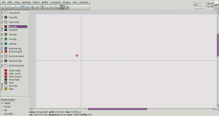
We begin by creating a hole for the centre of the footprint. We do this by selecting the via tool and placing a via at a suitable location in a new layout:


We place the via at (1000,1000) mil to simplify subsequent calculations:


We now select the via by clicking on it:


 We now use CTRL-x to cut the via to the buffer


We now use the "Convert buffer to padstack" menu item to convert the via to a padstack:


Having done so, we click to place the new padstack on the layout:


We now click on the padstack to select it:


Having selected the padstack, we can now invoke the padstack editor with the :padstackedit() command:


this produces the following window:


if we click on the prototypes tab, we can inspect and edit the characteristics of the padstack we have just created from the via. We begin by setting the diameter of the hole to 0.222 in, based on the electron tube data sheet. Note that pcb-rnd understands common dimensional suffixes, like 'mm', 'nm', 'in' or 'mil':


We also note that there are superfluous copper shapes defined for the top, bottom and inner layers. This is to be expected, given that we made the padstack from a via. We can click on the "change..." button for the top layer copper shape to edit it:


We can delete the copper shape for this layer, and do the same for the other defined copper layer shapes. The final result is a padstack property window showing no copper shapes defined, as required for a simple hole:


Having sorted out the central hole for the footprint, we now use the via tool to place a new via that is to become the padstack used for the pins of the B7G tube.


Having done so, we select the via and with the top layer selected, we type ':shape()' to invoke the copper polygon shape tool...


which brings up the following window, allowing us to create a polygon that will become a pad for the padstack. We begin by editing the horizontal and vertical dimensions:


We then choose a more rounded pad shape, by increasing the number of corners to 10. Note that the shape() dialogue also supports the creation of round, rounded corner rectangle ("roundrect") and rectangular pads. Polygonal pads were chosen for this particular footprint because of the radial spacing and symmetry of the pins on the tube:


Having done this, we use the shape() tool to create another pad for our padstack on the bottom copper layer:


Having added to polygonal pads centred on our via, we use the selection tool to select the three features


which we then cut to the buffer  with CTRL-x


and proceed to convert to a padstack with the "Convert buffer to padstack" menu item:


We now place the padstack in an intended location,  based on the datasheet for the tube:


We continue pasting the padstack from the buffer in the remaining pin locations, based on the dimensions from the data sheet:


We place the easy 90 degree spaced pin padstacks first:


And then do a bit of trigonometry to calculate the positions of the remaining pins and place padstacks in these locations too:


Having positioned the padstack in the necessary locations, we review the work thus far:


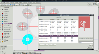
Our next job is to rotate the various padstacks as necessary. We do this by selecting each padstack in turn, using CTRL-e to invoke the property editor, and altering the rotation value as required. Applying -45 subtracts 45 degrees from the current value:


Similarly, applying 45 to the rotation, adds 45 to the rotation value:


Likewise, additional rotation of 90 is applied to the top pin:


almost done, we add 45 degrees rotation to the bottom left pin:


and we finish by subtracting 45 degrees rotation from the bottom right pin:


 We now select the arc tool....


And now select the top silk  layer to draw an arc to denote the outline of the tube, based on the datasheet:


A simple way to do this is to draw a 90 degree arc as follows:


after this, select the arc and invoke the property editor with CTRL-e to define the desired value for delta, to create a circle. The other way to do this is to simply click on the end of the arc and then drag the end of the arc around until a circle is formed.


The text tool is now used to add a text label to the footprint.


Having completed the components required for the thermionic valve, the set of features is selected: 


and CTRL-x is then used to cut the selection to the buffer. It is important to note that the location of the mouse when CTRL-x is used determines the origin of the resulting footprint. In this case, the cursor is snapped to the central hole before using CTRL-x, to give a footprint origin centred on the hole:


With the features now cut to the buffer, we can convert the buffer contents to a subcircuit with the menu item "Convert buffer to subcircuit":


We now see the red, thin dashed line surrounding our new footprint, labeled 'U0':


All that remains is to number the terminals of the footprint. This is done by hovering over a terminal, and typing 'n', which brings up a window allowing a label to be specified. Each of the pins is numbered this way.


The numbering can be checked afterwards by hovering over each pin in turn, and noting its properties:


We now inspect the completed footprint from the top


We inspect it from below, by hovering over the centre of the footprint and using SHIFT-Tab to flip the board


We return to the front view and see the effect of turning off 'Subcircuits' visibility, which toggles the display of the dashed thin red outlines of subcircuits


We also see the effect of turning off 'Padstack marks' visibility, which toggles the display of the red padstack crosshairs


We now undertake the final task of setting an appropriate solder mask clearance for the padstacks.
We select the footprint:


We now invoke the padstack editor with :padstackedit() to get the following window:


we click on the prototype tab to view the properties of the padstack upon which all seven pins are based


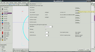
In this window, we see that there are no solder mask properties. We click on "change..." and automatically generate a mask shape for the top layer:


We now do the same for the bottom layer mask properties:


and automatically generate a mask opening:


While it is open, we also use the padstackedit() window to confirm, or change if necessary, that the pin holes have 40mil (0.040 in) diameters, as per the data sheet. Obviously, at this point, individual designers might opt for larger holes to allow some room for variation in manufactured pin sizes and PCB manufacturing tolerances.


Similarly, if a copper pad shape has been defined for the top layer, the padstackedit() window can be used as a short cut to copy the shape to the bottom layer, eliminating the need for manually creating a bottom layer shape for inclusion in a padstack being created from scratch.


We finish by toggling the solder mask layer, and seeing the resulting solder mask clearances:


In closing, we note that the preceding example demonstrates multiple new features in pcb-rnd:

1) Footprints are now subcircuits, rather than a distinct hardwired "element" type. This means that a text label or text labels are now possible within footprints, and also that an arbitrary polygonal pad is possible on any given layer, rather than the more limited options in the past of SMD (rectangular), round pins and square through hole pins.

2) the shape() tool is a quick and easy way to build common padstack copper features.

3) we saw how pcb-rnd can use a padstack prototype which can then be copied and modified as needed within a footprint. In this case, the one prototype padstack sufficed for all seven pins, the only differences between them being rotation.

4) holes are now just a type of padstack, and are no longer a unique or distinct feature type.