Sunday, 16 April 2017
Bitmap import now supported by pcb-rnd, including Easter eggs
Support for parametric footprints within pcb-rnd, the gEDA PCB fork, now allows on the fly insertion of any graphic file type as a silkscreen bitmap, including easter egg depictions, of course, that are supported by the netpbm package that the bitmap() script depends on.
At this point in time, netpbm supports:
bmp, fiasco, fits, gem, gif, jpeg, palm, ps, rast, rle, sgi, sir, tiff, xwd, zeiss, png
which means that any of these image formats can be inserted, on the fly, into a pcb-rnd PCB layout as a bitmap.
The bitmap() script can be found on the edakrill repository.
The script files need to be installed in the search path for parametric footprint elements, i.e.
pcb-rnd/trunk/pcblib/parametric/
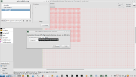
The footprint insertion dialogue is invoked with the usual "i" command, at which point the path to the image can be entered into the bitmap() footprint dialogue as follows, along with pixel size details:
At which point the graphic is turned into an element in the buffer:
Which can then be placed on the layout:
This is a somewhat simpler way of inserting images than other workflows including the use of pstoedit or image2footprint, previously described, which are used standalone to generate the layout element for subsequent insertion into the PCB layout.
Image size and resolution should be kept sensible, as the resulting footprint silkscreen elements will get quite big and bloat a layout if excessively high resolution images are used, and may encounter manufacturer limitations with minimum silkscreen dimensions, i.e. less than 6 or 8 mil, depending on the manufacturer.


No comments:
Post a Comment