Based on a set of example files supplied by a Mentor Graphics Design Capture user, import has been implemented following reverse engineering of the EDIF files supplied.
Of note, the importer does not use the old EDIF import code, relying instead on the s-expression parser library more recently developed for KiCad import.
The importer allows use of the native Mentor parts database, with a regex based translation table during import into pcb-rnd that translates Mentor's parts into pcb-rnd native footprint names. This can use any attribute of the input part and can generate the pcb footprint using parts of the input string,
e.g. there is a single rule that says if Part Name is Dummy_HDR 1x2 P:2.54mm, extract the "1x2" and the "P:2.54mm" sections and add attribute
footprint=connector(1, 2, 2.54mm)
which is a valid pcb-rnd parametric footprint.
This feature allows those using the Mentor Graphics Design Capture for schematic design to then layout a PCB in pcb-rnd based on the exported schematic netlist. The supported export netlist format is a flattened EDF file.
Options for further development and improvements include attempts to import mentor footprints (i.e. geometry), and possibly attempts to import hierarchic netlists, with subsequent flattening within pcb-rnd.
Starting with a Mentor Graphics Design Capture schematic
the next step is to generate a netlist for importing by pcb-rnd based on the Mentor Graphics Design Capture schematic; the first thing is to open the utilities menu
In this menu, the option for exporting a netlist in EDIF format can be selected. In particular, the flattened schematic option must be selected:
If successful, an EDIF format netlist should be written to your filesystem:
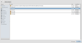
The next step is to load the netlist file within pcb-rnd:
It is at this point the footprints should be seen on the layout, and connections can be viewed with the rats nest optimize 'o' button:
from here, PCB layout proceeds as usual, with, of course, the option of adding additional footprints with the insert 'i' command.
In closing, the pcb-rnd project is keen to enable a variety of workflows and foster interoperability between layout and design tools. If you have a preferred schematic design tool, or are considering a move away from an existing tool and would like to see the ability to import legacy designs, feel free to get in touch with the developers on irc.


No comments:
Post a Comment